Gaojia Optotech
Some time ago, I received many inquiry orders from partners. Often only a surface accuracy value was provided, without specifying whether it referred to PV or RMS—this is very unrigorous.
Take an optical mirror with an inspection report stating: Surface Figure Error: PV = 0.2λ, RMS = 0.03λ
Now the question is: Is this mirror qualified for use?
If the supplier then says: "Our wavefront error is 0.06λ RMS."
Is this the same specification as above?
The answer is no, and there is actually a full 2x difference between them.
In practice, these two concepts are frequently confused—not only by newcomers to the optics industry, but even by senior technicians with ten years of optical processing experience.
More importantly, this is not merely a theoretical confusion. It can directly lead to production failures, contract disputes, and even full batch scrappage of products.
I once heard of a real-world dispute case.
An optical factory received an order for primary mirrors for astronomical telescopes. The customer specified the requirement: Surface figure better than λ/10 (wavelength: 632.8 nm).
The factory completed processing as usual, and the interferometer test results were as follows:
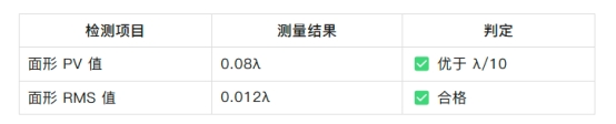
With this test result, the factory shipped the products with full confidence.
However, after the customer received the mirrors and tested the system wavefront on the complete optical assembly, the outcome was disappointing: The Strehl ratio was far below the design specification, and the star point image became severely blurred, making the mirrors completely unusable.
A dispute immediately broke out between the two parties.
The factory argued: "The surface figure PV is 0.08λ, which is obviously better than your required 0.1λ. Where exactly are we non-compliant?"
The customer countered: "Your wavefront error is far from meeting the standard, nowhere close to the λ/10 requirement!"
So where lies the root cause?
The customer’s specification stated surface figure better than λ/10, but what they actually required in practice was wavefront error better than λ/10.
For this reflective primary mirror, the wavefront error is twice the surface figure error. As a result, both sides talked past each other with conflicting understandings, and the entire batch of lenses was returned.
Now let’s clarify these concepts thoroughly once and for all.
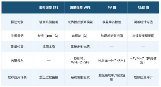
1. Surface Figure Error / Surface Form Error
Surface figure error refers to the deviation between the actual geometric profile of an optical surface and its ideal designed shape.
Simply put: Treat the mirror as a 3D curved surface. An interferometer emits a reference beam to compare the actual surface with an ideal spherical or flat surface; the resulting deviation value is the surface figure error.
Surface figure error is a pure geometric quantity that only describes the mirror surface itself. It is independent of the light source, as well as whether the light is reflected or transmitted.
Measurement tools for surface figure error: Interferometer (Fizeau interferometer, Twyman-Green interferometer), profilometer, wavefront sensor.
Common characterization parameters: PV (Peak-to-Valley) value, RMS (Root Mean Square) value, Zernike coefficient decomposition.
2. Wavefront Error
Wavefront error describes the deviation between the actual wavefront and the ideal spherical/plane wavefront after light propagates through an optical system.
It is a quantity related to optical propagation. Instead of representing the geometric property of a single surface, it is the comprehensive result after light passes through all optical elements in the system.
The core difference between wavefront error and surface figure error can be seen in this classic question: If a mirror has a surface figure error of λ/20, what is the wavefront error it introduces?
The answer is λ/10 — exactly doubled.
The reason is straightforward: Light strikes the reflective mirror once on incidence and once upon reflection, traveling two optical paths. Thus: Wavefront Error = 2 × Surface Figure Error
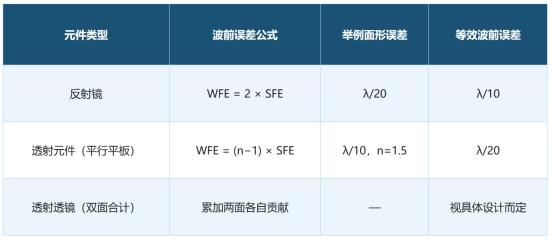
where n stands for the refractive index, typically ranging from 1.45 to 1.9 for optical glass. SFE denotes Surface Figure Error, and WFE denotes Wavefront Error.
3. PV vs RMS — Stop Mixing Them Up
After distinguishing surface figure error from wavefront error, we need to clarify another pair of easily confused indicators: PV and RMS.
Both are statistical descriptions of error distribution, but they focus on completely different aspects.
PV (Peak-to-Valley)
PV value = The highest error point minus the lowest error point within the full aperture.
Advantages: Intuitively reflects the worst-case condition; highly sensitive to isolated defects and edge warping.
Disadvantages: Easily distorted by individual abnormal points, and cannot represent the overall surface quality.
RMS (Root Mean Square)
RMS value is calculated by squaring the error of each sampling point over the full aperture, averaging the squared values, then taking the square root.
Advantages: Clear statistical significance, reflects the overall machining quality, and has a direct correlation with the Strehl ratio.
Disadvantages: Insensitive to individual local defects; relying solely on RMS may conceal local high spots.
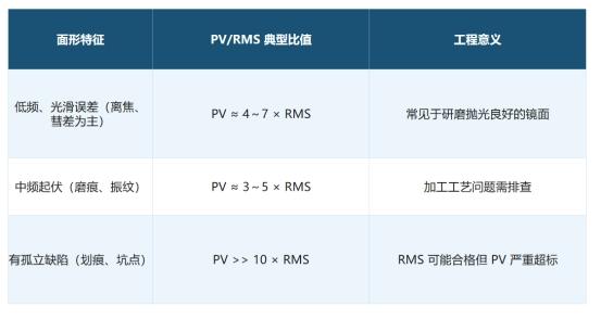
Relationship between PV and RMS
There is no fixed proportional ratio between PV and RMS.
Many practitioners follow the empirical formula: \(\text{RMS} \approx \text{PV}/5\). This rule is only valid for optical surfaces with smooth, low-frequency error distributions.
Conclusion: A test report is complete only when both PV and RMS are provided. Relying solely on either one is one-sided.
We can clearly visualize the relationship among these indicators with a table.
Now, I’ll share three practical questions for reading optical inspection reports. This avoids discrepancies between processing results and actual requirements caused by inconsistent understanding, as well as subsequent disputes.
The next time you receive an optical inspection report, ask yourself these three questions first:
1. Is this surface figure error or wavefront error? (Determines whether numerical conversion is required)
2. Is the given value PV or RMS? (The two can differ by 4~7 times and must never be confused)
3. Which parameter does the specification correspond to? (Contract terms must match measured parameters one-to-one)
Here are common reference specifications (visible light band, λ ≈ 633 nm) for quick intuitive judgment:
· General precision optical components: Surface figure PV < λ/4, RMS < λ/20
· High-precision astronomy & laser optics: Surface figure RMS < λ/50, Wavefront RMS < λ/20
· Ultra-precision applications (EUV, gravitational wave detection): Surface figure RMS < λ/1000, converted to nanometer or picometer scale.
IV. Closing Remarks
Optical processing, inspection, and optical design are three separate professional fields, yet they rely on the same inspection reports for daily communication.
Surface figure error is the language of optical processing technicians; wavefront error is the language of system engineers; PV and RMS are the language of statistical mathematics.
Mixing these three "languages" makes problems inevitable—smooth cooperation is merely accidental.
It is hoped this article helps you build a clear logical framework. From now on, you will no longer feel confused or make guesses when reading optical inspection reports.Article Source: Official Account · Deep Optics Insight